DC Boost Voltage Regulators
The world’s first efficient switching-free boost regulator — linear-regulator simplicity and noise, with boost functionality and no inductor.
Features
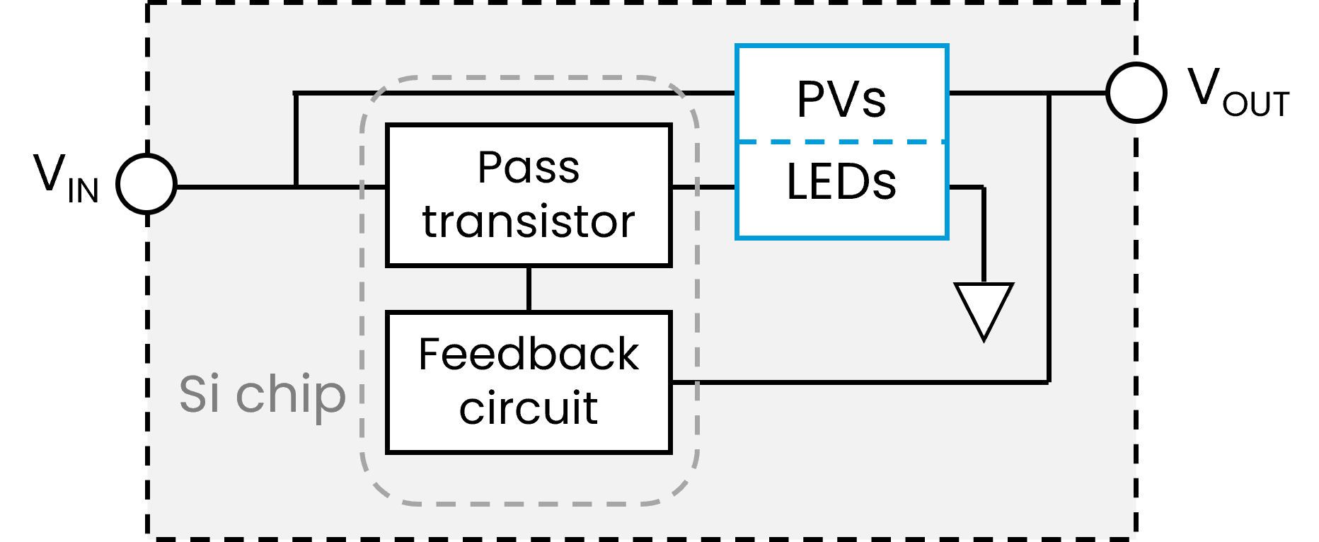
Polaris Semiconductor’s pioneering technology enables DC power management with the low noise, compactness and simplicity advantages of linear regulators but with dramatically higher efficiency — as well as boost functionality. This entirely linear technology eliminates the EMI effects associated with switching alternatives, simplifying circuit design, PCB layout and reducing the risk of a costly redesign. The inductorless, switching-free topology uses photons generated within proprietary optocoupler chips to boost the input voltage with high efficiency, simplifying thermal design and reducing electrical losses without introducing noise and footprint tradeoffs.
A new class of boost converter
Pure DC boost regulation
The world’s first efficient switching-free boost regulator. Typically >65% peak conversion efficiency — bringing linear-regulator simplicity, low noise, and minimal BoM to the realm of boost converters.
Ultra-high PSRR & low noise
A proprietary photonic technology delivers the clean, ripple-free output of a linear regulator at much higher efficiency, matching the noise specs of the best available LDOs while reducing solution size, BoM and design complexity.
Minimal footprint and BoM
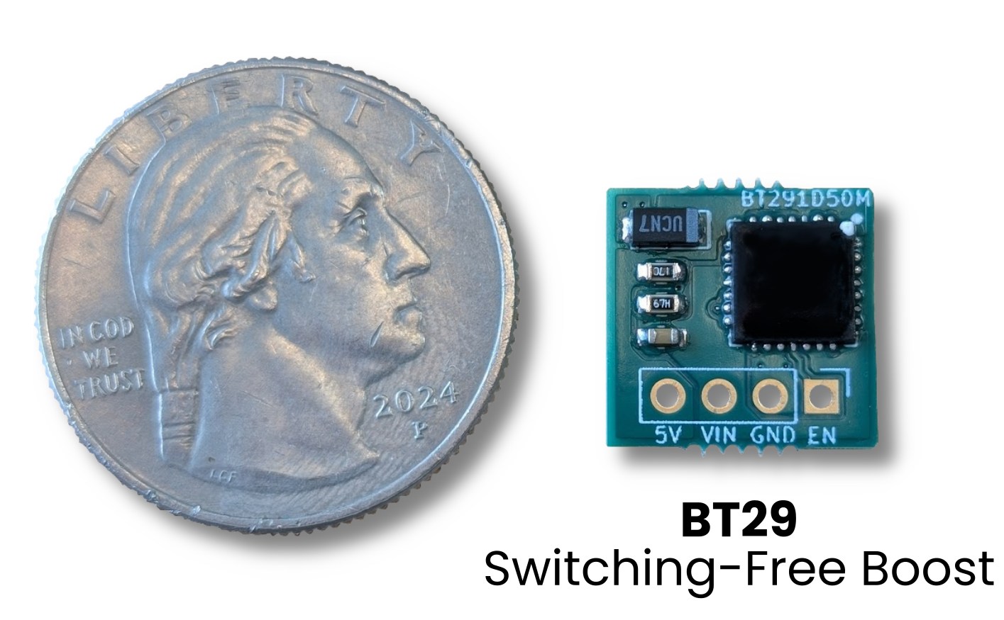
No inductors and only a handful of small passives. Compact QFN packages (36–49 mm² area, 0.8 mm profile) ideal for space-constrained applications with demanding power-integrity requirements.
Boost family
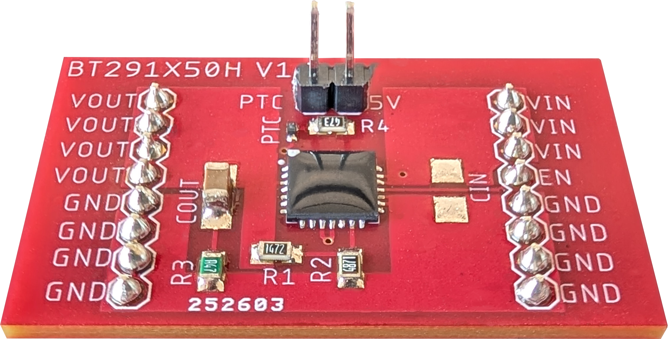
We currently offer one family of boost DC voltage regulators. Key performance attributes are summarized below. Full datasheets are available on request, and all products are available on evaluation boards. If you don’t see a product that suits your application, get in touch — we also offer custom designs.
| Device family | Max Iout (mA) | Min Vin (V) | Max Vout (V) | PSRR @ 1 kHz | TID krad(Si) |
|---|---|---|---|---|---|
| BT29 | 500 | 3.1 | 5 | 60 dB | 200 |
- Minimum input voltage is specified at Iout = 0.1 A in optocoupler-enhanced mode.
Reading a Polaris part number
Output-voltage code (buck): 18 ⇒ outputs up to 2 V · 33 ⇒ up to 4 V · 50 ⇒ up to 5 V (up to 6 V on BK301D50H). Outputs are adjustable: BK19 and BK29 devices down to 1.2 V, BK30 devices down to 0 V — see the selection table for each part's exact range.
Input-voltage range: L lowest · M medium · H high · E extended — IDs ending in V select between two ranges via board-level pin connections. Every device also runs as a conventional LDO by shorting two pins ("LDO mode").
Boost (BT) parts share the same grammar but regulate up to 5 V — see the BT29 series page for output behavior.
Boost without switching
Our boost voltage regulators feature a high-performance low-dropout (LDO) linear regulator IC, co-packaged with our patented high-efficiency PV-output optocouplers. The photovoltaic array boosts the output voltage above the input voltage without switching. The device retains the advantages of conventional LDOs — tightly regulated, low-noise output, highly effective input ripple rejection, a small footprint and component count, and robust protection and functionality features.
Application optimization
In precision instrumentation, low-noise analog circuits, and RF systems, our boost regulators provide essential voltage-boost capability without introducing switching noise. They offer an elegant solution wherever engineers need boost functionality without the complexity and EMI challenges of switching regulators. The minimal bill of materials and straightforward implementation make them especially attractive for space-constrained designs and projects prioritizing simplified power management.
Go deeper on boost ELRs
Ready to design it in?
Request evaluation samples, detailed datasheets, and SPICE models — an engineer answers, not a sales funnel.