Designing a Switching-Free Boost Regulation and Battery Charging Solution for Single-Cell Li-Ion
Introduction
A vast range of electronic devices use single cell Li-ion batteries for power. Compared to multiple cell approaches, single-cell designs offer compactness, simplicity, cost and reliability advantages. If a system requires voltages greater than that available from a single Li-ion cell, then designers usually opt to use boost converters rather than multiple-cell configurations. However, boost converters can create some difficult design challenges, especially if the system has demanding noise and size specifications. Switching regulators are a source of electrical noise that can be both conducted to downstream components and radiated to other areas of a system. Dealing with this can introduce major tradeoffs in performance, footprint, bill of materials, efficiency, cost and EMC risk. In this application note, we describe the design of a switching-free boost and Li-ion battery charging solution that can overcome the drawbacks associated with switching solutions. We demonstrate a compact, simple, all-linear design suitable for generating a low noise 5 V rail and charging circuit in a single-cell Li-ion equipped system. This uses Polaris Semiconductor’s unique, switching-free boost converter technology, combined with a high-performance linear battery charger IC from Texas Instruments.

BT291D50M Boost Converter
This application note leverages Polaris Semiconductor’s optocoupler-enhanced linear regulator technology for boost conversion. This patented device architecture comprises a conventional, Si-based LDO, co-packaged with our unique, high-performance, GaAs-based photovoltaic-output optocouplers in a multi-chip QFN package. The role of the optocouplers is to transfer optical power from the LED section to the photovoltaic (PV) devices with high efficiency.
With the boost-converter configuration of BT291D50M (Figure 1), the LDO supplies current to two series-connected LED devices, which is efficiently transferred to photocurrent in the two PV devices via photons emitted in the LEDs. The PV devices are connected to the input and output terminals of the regulator, enabling the output voltage to exceed the input voltage. The maximum power voltage of each PV element is roughly 1 V, and therefore the device configuration shown can efficiently boost the output voltage by up to 2 V greater than the minimum input voltage at which the device turns on.
A regulated output is achieved using a feedback loop around the LDO error amplifier. A scaled representation of the output voltage is sensed at the ADJ pin, tied to the center of a resistor divider that connects OUT and GND. The error amplifier of the LDO controls the current supplied to the LED elements via the pass transistor, generating current in the PV array that is supplied to OUT. The feedback loop around the error amplifier acts to compensate any difference in the reference voltage and the voltage at the ADJ pin, thus regulating the output voltage. The minimum input voltage of the device () is the sum of the forward voltage of each LED and the dropout voltage () of the LDO. The forward voltage of the LEDs is typically 1.3–1.6 V, depending on current, and is approximately 250 mV at the maximum rated current. Therefore, BT291D50M is well suited for generating a 5 V output from typical Li-ion battery voltages in the 3.4-4.2 V range. For a more complete discussion of optocoupler-enhanced linear regulators, consult our white paper PSWP001 [1].


The high efficiency of Polaris Semiconductor’s optocoupler chips allow overall voltage regulator device efficiencies in the 50%–68% range to be achieved for a 5 V output. Figure 2 shows the output voltage and efficiency for BT291D50M with a 50 mA load, with of roughly 2.9 V. The increasing forward voltage and LDO dropout voltage with higher currents results in increasing to approximately 3.5 V at the maximum load current of 350 mA and 25 °C (Figure 3).
Of course, the efficiency of BT291D50M is lower than a high efficiency switching regulator, but there are several key advantages to the linear topology that make it attractive. Firstly, no switching means that the traditional drawbacks of output voltage ripple and conducted and radiated electromagnetic interference (EMI) are avoided. In sensitive analog and RF systems, designers often go to great lengths to suppress switching noise artifacts that can degrade fidelity and introduce PCB design risks. The second advantage is that the device retains the high power-supply ripple-rejection (PSRR) performance of an LDO, and therefore not only does BT291D50M not introduce switching noise into the system, but it can also reduce noise from a dirty supply. Finally, the device can offer significant BoM savings—using linear post regulators and filters to clean the output of a switching regulator in noise-sensitive systems results in degraded efficiency, higher component count, increased cost, lower reliability, and potential instability. The passives required by switching regulators can occupy significant volumes, whereas the inductor-less linear topology operates with a very small number of passives.
All-Linear Li-Ion Charger & Boost Regulator
In this application note, we describe using BT291D50M in Li-ion battery-containing systems in combination with a battery charger IC. Using this approach it is possible to generate a ripple-free 5V rail to power sensitive loads with power sourced either from a line input or directly from the battery, as well as charge the battery when required. BQ25185 is a linear battery charger IC produced by Texas Instruments with numerous attractive features for this application, including low quiescent current, up to 1 A charging current, a wide range of fault protection features, power-path management functionality and input voltage dynamic power management for high impedance input sources such as solar panels. Moreover, the all-linear architecture of BQ25185, combined with the linear boost capability of BT291D50M, means no inductors are required and no switching noise is generated anywhere within the circuit, simplifying PCB layout design and eliminating EMI risks associated with integrating power management into sensitive analog circuits.
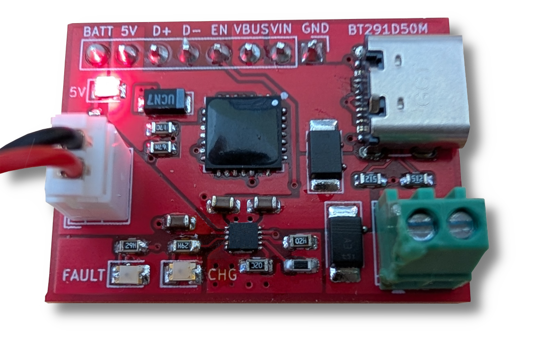
A photo of the linear boost and battery charger demonstration board is provided in Figure 4. Figures A1–A3 show the schematic, and Table A1 provides the complete bill of materials. Inputs to BQ25185 can either be from a USB connector with nominally 5 V input (J3), or a line input (J2) up to 18 V maximum. A power multiplexer is not used in the demonstration, so instead Schottky diodes (D1 & D5) are included on both inputs to prevent reverse current flow in either input channel. In the presence of a high enough VIN, BQ25185 (U2) outputs a regulated system voltage VSYS of 4.5 V. This is then supplied to the BT291D50M (U1) device which is configured for a 5 V output to power system loads, set by resistors R1 and R2. The VSEL pins of the device are tied together, connecting the internal LED elements in series.


Additional input current is drawn by BQ25185 to charge the battery, if connected, with a configurable charge profile: the maximum input current and battery regulation voltage is controlled by an off-chip resistor, R6, and the fast charge current is set using an additional resistor, R3. In this example, the charge current is set for 300 mA, the maximum input current (ISET) is 500 mA, and the battery regulation voltage (VSET) is 4.2 V. If the battery voltage falls between the low battery voltage set point and VSET, the battery is charged in constant-current mode, and transitions to constant-voltage mode when the battery voltage reaches VSET. More detailed information on the configuration and operation of BQ25185 can be found in the datasheet for this part [2].
If the line input is disconnected when a battery is present, the system voltage VSYS is supplied directly from the battery, provided the battery voltage is above the battery voltage under voltage lockout threshold. In this mode, the boost regulator maintains a regulated 5 V supply to the load as long as VBAT exceeds the minimum of BT291D50M, see Figure 3. Generally, the nominal voltage for a lithium-ion battery is close to 3.7 V during most of the discharge process, which is well suited for the BT291D50M input range.
Three indicator LEDs are included in the design. LEDs D2 and D3 are tied to STAT1 and STAT2 pins, with detailed functionality described in the BQ25185 datasheet [2]. Briefly, D3 illuminated and D2 extinguished indicates charging is in progress, D2 illuminated and D3 extinguished indicates a recoverable fault condition, both D2 and D3 illuminated indicates a non-recoverable fault condition, and D2 and D3 extinguished indicates either charge complete, charging disabled or sleep mode. LED D4 is illuminated when BT291D50M output is high. The component placement, front and rear copper designs for a two-layer demonstration board are provided in Figure 5. The total board size of the demonstration PCB is 31.8×23.4 mm². The layout of BT291D50M and its passives is based upon that described in our application note PSAN001 [3], which shared a PCB design for this chip with a miniscule solution size of 12.5×7.5 mm².
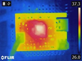
The performance of the design under typical operating conditions has been tested experimentally by assembling the circuit on a 2-layer PCB with 1 oz (35 µm thickness) copper. A fixed load resistance of 100 Ω was attached to the boost regulator output, resulting in a load current of approximately 50 mA. During testing, the board was in a room temperature environment with only natural convection and no forced cooling applied. To simulate battery-only operation, a DC power supply voltage of 3.7 V was connected to J4. In this mode, the linear boost converter was dissipating approximately 177 mW of power, and outputting 249 mW of power to the load resistor. The package temperature of the boost regulator was measured to be 38.9 °C using a FLIR camera, shown in Figure 6a.
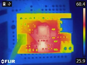
The circuit was also tested in charging mode by connecting a line input voltage of 5 V to J2 and an SMU to the battery connector. The SMU was sinking a charge current of close to 300 mA at the simulated battery voltage of 3.7 V. This configuration dissipated 275 mW of power with a total output power of 368 mW split between the battery and load. The greater power dissipation raised the board temperature, with package temperatures of BQ25185 and BT291D50M measured to be 65.7 °C and 58 °C, respectively, shown in Figure 6b. These package temperatures are well within the limits of both devices. A summary of the electrical performance of the demonstration board in both modes is provided in Table 1.
| Battery Power | Charging + Load | |
|---|---|---|
| IIN (mA) | 0 | 427.0 |
| VIN (V) | 0 | 5.00 |
| IBAT (mA) | 115.1 | −298.2 |
| VBAT (V) | 3.70 | 3.70 |
| IOUT (mA) | 49.9 | 50.0 |
| VOUT (V) | 4.99 | 4.99 |
| Efficiency (%) | 58.4 | 63.3 |
Summary
Polaris Semiconductor’s linear boost regulator devices offer a very compact and low-noise solution for boost conversion. Conventional switching approaches inevitably generate conducted and radiated EMI concerns that require careful PCB layout and filtering, which can introduce major performance risks and design trade-offs in noise-sensitive analog and RF circuits. By combining the linear boost converter with a linear battery charger IC, it is possible to achieve a compact, efficient, inductor-less solution that is entirely switching-free, perfect for battery powered systems that have demanding low-noise requirements such as medical wearables, remote and portable sensors, RF transceivers and many more.
Appendix
Li-Ion Battery Charger Schematic


Li-Ion Battery Charger Bill of Materials
| ID | Description | Part | Manufacturer |
|---|---|---|---|
| C1, C3, C4 | 10 µF ceramic X7R | GRM188Z71A106MA73D | Murata Electronics |
| C2 | 33 µF tantalum poly. | T527S336M016ATE200 | Kemet |
| D1, D5 | Schottky Barrier Rectifier | PMEG3020ER | Nexperia USA Inc. |
| D2, D3, D4 | Red LED | B1701URO-20D000114U1930 | Harvartek Corporation |
| J1 | 8-Pos. Vert. Header | 61300811121 | Wurth Elektronik |
| J2 | 2-Pos. Terminal Block | VN02A1500000G | Amphenol Anytek |
| J3 | USB 2.0 TYP C Receptacle | USB4105-GF-A | GCT |
| J4 | 2-Pos. Vert. Header | S2B-PH-K-S | JST Sales America Inc. |
| R1 | 14.7 kΩ 0.5% 1/16W | RR0816P-1472-D-17C | Susumu |
| R2 | 4.87 kΩ 0.5% 1/16W | RR0816P-4871-D-67H | Susumu |
| R3 | 1.02 kΩ 0.5% 1/16W | RR0816P-1021-D-02H | Susumu |
| R4, R5 | 1.96 kΩ 0.5% 1/16W | RR0816P-1961-D-29H | Susumu |
| R6 | 18 kΩ 1% 1/10W | ERJ-3EKF1802V | Panasonic |
| R7, R8 | 5.1 kΩ 1% 1/10W | RC0603FR-075K1L | Yageo |
| R9 | 10.2 kΩ 0.5% 1/16W | RR0816P-1022-D-02C | Susumu |
| R10 | 2.32 kΩ 0.5% 1/16W | RR0816P-2321-D-36H | Susumu |
| U1 | 5V Linear Boost Regulator | BT291D50M | Polaris Semiconductor |
| U2 | 1A Li-Ion Linear Battery Charger | BQ25185DLHR | Texas Instruments |
References
- M. P. Lumb et al., “Breaking the rules of linear regulators: High efficiency buck and boost conversion without switching.” Polaris Semiconductor; White Paper PSWP001, 2025. Available: https://www.polarissemiconductor.com/techdocs/#WP
- BQ25185 1-cell, 1-A standalone linear battery charger with power path, factory mode, and battery tracking VINDPM. Texas Instruments; Datasheet SLUSF65, 2023.
- K. J. Schmieder and M. P. Lumb, “Switching-free boost regulators: A compact, all-linear solution to stepping-up voltage.” Polaris Semiconductor; Application Note PSAN001, 2025. Available: https://www.polarissemiconductor.com/techdocs/#PSAN001
Ready to design it in?
Request evaluation samples, detailed datasheets, and SPICE models — an engineer answers, not a sales funnel.