Designing for Multiple Power Sources: Seamless Performance Optimization with Enhanced Linear Regulators
Introduction
Portable electronics demand ultra-low noise power delivery to sensitive analog circuits. These products increasingly operate from dual power sources—USB connectivity for stationary use and internal batteries for portability—creating a fundamental challenge for power management design. The regulator must deliver stable, low-noise output voltage while efficiently handling input sources that vary from 3.5 V (Li-Ion battery) to 5 V (USB power).
This application note presents an adaptive dual-mode regulation technique that maintains the noise performance and simplicity of linear regulation while achieving high efficiency across the full input voltage range. The approach uses a single Polaris Semiconductor enhanced linear regulator (ELR) to eliminate the conventional two-stage buck-plus-LDO architecture, reducing cost, board area, and design complexity while delivering superior performance in noise-critical applications.
The Challenge
Consider a portable precision instrument such as a spectrum analyzer, data acquisition unit, or signal conditioning system. In these products, supply noise directly limits measurement accuracy and system dynamic range. Such instruments typically require a stable 3.3 V supply with noise performance in the low microvolt range.
Linear regulators offer a compelling solution for providing a clean, stable 3.3 V rail from a single-cell Li-Ion source. Since their efficiency is largely dictated by the ratio of output to input voltage, these regulators can achieve upwards of 85% efficiency when stepping down from 3.7 V (nominal battery voltage) to 3.3 V, while simultaneously offering extremely low output noise and a remarkably compact footprint. The topology is straightforward: a series pass element and feedback network with minimal external components—typically just input and output capacitors. For battery-powered operation, this represents an effective solution combining high efficiency, zero switching noise, small size, and low cost.
When the power source switches from battery to USB, however, the higher 5 V input voltage creates a substantial efficiency penalty. The same linear regulator now operates with a 1.7 V drop across the pass element, reducing efficiency to the range of 60%–65%. For a typical portable instrument drawing 500 mA at 3.3 V output, the regulator must now dissipate 900 mW as heat when powered from a 5 V USB source—more than tripling the thermal load compared to battery operation (see Figure 1). This heat dissipation creates thermal management challenges in compact enclosures, forces reduced battery charging rates, and in some cases requires limiting output power to prevent thermal shutdown.

The straightforward response to this efficiency problem is to avoid using linear regulators when the input-output differential becomes large. Switching regulators can handle the 5 V to 3.3 V conversion with 85%–90% efficiency, making them the standard choice for USB-powered operation. However, their switching noise conflicts with the noise requirements of precision analog circuitry. This tension between efficiency and noise performance has driven many designs toward a compromise approach.
To address this dilemma, designers often opt for a two-stage power architecture: a buck switching regulator handles the primary conversion from 5 V down to an intermediate voltage (3.8–4.3 V), followed by an LDO that provides the final step to 3.3 V while filtering switching noise. This achieves a respectable overall efficiency of 70%–75% from 5 V input while maintaining adequately low output noise.
This two-stage approach, however, carries significant overhead. The buck converter requires an inductor, controller IC, compensation network, and EMI-aware layout with ground plane partitioning—all of which expand board area and design complexity. Even with proper filtering, switching harmonics can reach the output and create intermodulation products with sensitive signals. For noise-critical applications, the switching pre-regulator is a thermal necessity rather than an optimal solution.
The ELR Approach
Polaris Semiconductor’s enhanced linear regulators (ELRs) address this problem at its root. Rather than adding a switching pre-regulator to compensate for the LDO’s efficiency limitation, ELRs use integrated GaAs photovoltaic-output optocouplers to recycle energy that a conventional LDO would dissipate as heat. The result is a linear regulator that exceeds the conventional / efficiency ceiling—without introducing any switching noise.
For dual- and variable-source applications, a single ELR can operate in two modes—an optocoupler-enhanced mode for higher input voltages and a conventional bypass mode for lower input voltages—automatically selecting the optimal mode based on input voltage. This adaptive approach delivers the noise performance of a standalone LDO, the efficiency advantages of a two-stage architecture, and the simplicity of a single-device solution. Table 1 summarizes the comparison.
| Parameter | LDO | Buck + LDO | Adaptive ELR |
|---|---|---|---|
| 3.7 V Efficiency | High | Med-High | High |
| 5.0 V Efficiency | Low | Med-High | Med-High |
| Output Noisea | <1 µVRMS | Filter-dependent | <1 µVRMS |
| Switching Content | None | Present | None |
| Component Count | Low | High | Low |
| Board Area | Small | Large | Small |
| Design Complexity | Low | High | Low |
- a 10 Hz–100 kHz
The remainder of this application note explains how the two ELR operating modes work, describes a demonstration circuit that switches between them automatically, and presents measured efficiency, transient, and thermal performance across the full input voltage range.
How Enhanced Linear Regulation Works
While any of Polaris Semiconductor’s step-down enhanced linear regulators can be applied to multi-input performance optimization, this application note uses the BK301D33L for demonstration purposes. The device co-packages proprietary GaAs photovoltaic-output optocouplers with the Analog Devices LT3045, selected for its exceptional noise performance in precision analog applications. BK301D33L retains these best-in-class noise and power supply ripple rejection (PSRR) properties (see Figure 2), while significantly improving the electrical efficiency. The ELR technology is described in detail in white paper PSWP001 [1]; this section provides the conceptual overview needed to understand the adaptive dual-mode design.


Optocoupler Energy Recycling
In a conventional LDO, all input current flows through the series pass element and exits at the output. The voltage difference between input and output, multiplied by this current, is dissipated as heat. The efficiency ceiling is therefore / 66% for a 5 V to 3.3 V conversion.
The BK301D33L breaks this ceiling by providing a parallel current path through integrated optocouplers. Input current passes through an internal LED array, generating photons that photovoltaic (PV) cells capture and convert back to electrical current. This recycled current flows directly to the output, supplementing the current delivered through the pass element. Because the PV cells deliver current directly to the output, the regulator’s input current is less than the load current—the balance is supplied by the optocoupler path. The optocouplers achieve current transfer ratios exceeding 70%, enabling them to recycle a substantial fraction of the energy that would otherwise be lost as heat. However, the forward voltage of the LED array increases the minimum input headroom required for regulation—a trade-off that motivates the two operating modes described next.

Enhanced Mode vs. Bypass Mode
Figure 3 shows the device architecture and how the two operating modes are implemented. The BYP pin connects internally to both the collector of the pass transistor as well as the anodes of the LED array, while the LED cathodes connect to the output pin. On the photovoltaic side, four devices are configured in series with their positive terminal at OUT,PV and their negative terminal at ground. This internal topology enables the device to operate in two distinct configurations through external pin connections.
Enhanced Mode. OUT and OUT,PV are connected together while an external switch between BYP and OUT remains open. Current flows through the LED array, generating photons that the PV cells convert to useful current supplementing the output. The device can be operated in this mode permanently through a fixed pin configuration (by floating BYP and connecting OUT to OUT,PV), or switched into this mode dynamically—as demonstrated in this application note.
However, enhanced mode imposes a minimum input voltage requirement. The voltage dropped across the LED array, combined with the LDO’s dropout voltage and the output voltage, establishes a threshold below which enhanced mode cannot regulate. For the BK301D33L producing 3.3 V output, this threshold is in the range of 4.6–5 V depending on load current (see Figure 6). Enhanced mode is therefore well-suited for USB power at 5 V but cannot support Li-Ion battery operation (for = 3.3 V).
Bypass Mode. The external switch closes to connect BYP directly to OUT. This shorts the LED array and configures the pass transistor to drive the output directly, just as in a conventional LDO. The PV cells no longer contribute current, and the device operates with the low dropout characteristics of a traditional linear regulator. Efficiency in this configuration follows the familiar / relationship. Bypass mode operates efficiently at input voltages as low as 3.5 V (for = 3.3 V), making it appropriate for Li-Ion battery operation throughout the discharge curve.
The adaptive approach combines both modes: bypass mode at low input voltages where it operates efficiently, and enhanced mode at high input voltages where it recaptures energy that would otherwise be wasted as heat. The following sections describe the circuit that achieves this automatic transition and present measured performance across the full input voltage range.

Adaptive Dual-Mode Implementation
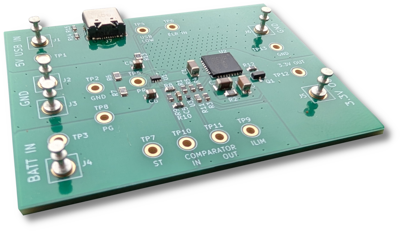
The flow diagram (Figure 4), demonstration board (Figure 5), and schematic in Figure A1 implement automatic mode switching based on the input voltage, allowing the regulator to seamlessly optimize efficiency as the power source changes between battery and USB.
The control circuit consists of three main functional blocks (Figure 4): input source selection with threshold detection, operating mode threshold detection, and MOSFET load switching. Proper selection of switching thresholds requires understanding the relationship between input voltage, load current, and the regulator’s operating modes.
Operating Boundaries
Figure 6 illustrates the key voltage thresholds and operating boundaries for the BK301D33L in this application. Two distinct threshold detection circuits govern the system’s behavior: one internal to the power multiplexer () that determines input source selection, and one external () that determines whether the regulator operates in bypass or enhanced mode.
The curve labeled ELR in Figure 6 represents the minimum input voltage at which the enhanced linear regulator can maintain output regulation at a given load current (25 °C operation). This threshold increases with load current because higher currents require greater forward voltage across the internal LED array, in addition to increasing LDO dropout voltage. At 50 mA, ELR is approximately 4.6 V; at 500 mA, it rises to nearly 5.0 V. If the input voltage falls below ELR while in enhanced mode, the regulator enters dropout and the output voltage decreases—behavior analogous to a conventional LDO operating with insufficient input voltage.
The threshold also varies with temperature. At 300 mA, BK301D33L measurements show decreasing at approximately −0.36 mV/°C, corresponding to a shift of approximately ±9 mV over a 0 °C to 50 °C operating range. This variation is modest but should be accounted for when selecting the operating mode switching threshold. As the relationship varies with load current, consult our datasheets or speak with an application engineer to determine the appropriate margin for your operating conditions.

The curve labeled + represents the minimum input voltage for bypass mode operation: the sum of the 3.3 V output and the pass element dropout voltage. This threshold is less sensitive to load current, remaining in the range of 3.5–3.7 V across the full load range.
Input Source Selection (THMUX)
Input source management is handled by the TPS2117 (U1) from Texas Instruments [2], a power multiplexer that automatically selects between two input sources. The device features an internal comparator that can be connected to the USB input through a voltage divider. When the USB voltage exceeds the internally-set threshold ( in Figure 6, approximately 4.5 V), the multiplexer switches from battery to USB power. This threshold-based approach ensures the multiplexer selects USB power only when the USB source is capable of supplying the load. The TPS2117 transitions smoothly between sources following a sub-20 µs break-before-make switchover delay, making it appropriate for applications where both sources may be present simultaneously, such as when a portable device charges while in use. The selected input voltage then feeds the BK301D33L regulator and the operating mode selection circuit.
As shown in Figure 6, is set below ELR across the full load current range. This means the system may briefly operate from USB power in bypass mode before the input voltage rises sufficiently to enable enhanced mode operation.
Operating Mode Selection (THCOMP)
The second threshold detection circuit uses a precision comparator (U3, TLV4041R1 from Texas Instruments [3]) configured with an external resistive voltage divider to determine when the input voltage crosses the boundary between bypass and enhanced operating modes. The shaded band labeled in Figure 6 indicates this threshold, including its hysteresis.
The divider network formed by R9 (31.6 kΩ) and R10 (10.2 kΩ) scales the input voltage down by a factor of approximately 4.1:1. This scaled voltage is compared against the TLV4041’s internal 1.2 V reference for state switching. The part features 20 mV of built-in hysteresis: the low-to-high transition occurs at 1.2 V, while the high-to-low transition occurs at 1.18 V. With the specified divider ratio, this translates to nominal switching thresholds of 4.92 V (rising) and 4.84 V (falling). In practice, the transitions were found to occur at 4.90 V (rising) and 4.83 V (falling), well-within the tolerance range of U3 and the associated passives (see Figure 7).
For reliable operation, must be set above ELR at the maximum expected load current. As shown in Figure 6, the demonstration circuit’s comparator threshold of approximately 4.9 V provides adequate margin for maximum load currents below approximately 300 mA. Applications requiring higher load currents would need to raise accordingly, though this reduces the input voltage range over which enhanced mode is active. Conversely, applications with lower maximum load currents could reduce to extend enhanced mode operation to lower input voltages.

The comparator sensing network (R9/R10) draws approximately 120 µA from the input at 5 V. As discussed in the Component Selection section, this divider can be resized with higher-value resistors to reduce current draw at the expense of increased mode-switching delay.
For applications requiring different operating mode threshold voltages, the divider ratio can be adjusted by changing R9 and R10 values. The threshold voltage is given by:
where is the comparator’s internal reference: 1.2 V for the positive-going input threshold and 1.18 V for the negative-going input threshold. To simplify the design, the comparator—as well as the power mux—is powered from the same rail that it monitors, eliminating the need for an additional supply.
Design Considerations for USB Voltage Tolerance
Standard USB bus voltage is specified as 4.75 V to 5.5 V [4]. At higher load currents, the ELR’s required headroom () may exceed the lower bound of this tolerance (4.75 V). The demonstration circuit thresholds are optimized to maximize Enhanced Mode efficiency for sources maintaining ≥ 4.9 V under load. For input voltages below this threshold, the device automatically transitions to Bypass Mode to maintain regulation. Designers wishing to extend Enhanced Mode operation to lower input voltages may adjust the resistive divider network to lower the switching threshold (), accepting that the maximum supportable load current in Enhanced Mode will be reduced.

| Input current (mA) | ||
|---|---|---|
| @ VIN=3.7 V | @ VIN=5.0 V | |
| Conventional LDO | 208 | 208 |
| Enhanced Mode ELR | n/a | 180 |
| Adaptive ELR | 208 | 180 |
Load Switching
The comparator drives a P-channel MOSFET switch (Q1, DMG2305UX-7) that controls the connection between the BYP and OUT pins. The TLV4041 features a push-pull output that actively drives both high and low states. When operating from battery power at approximately 3.7 V, the scaled voltage at the comparator’s input remains below 1.2 V, causing the comparator output to drive low. This pulls the gate of Q1 negative relative to its source, turning the P-channel MOSFET on and connecting BYP to OUT to engage bypass mode. When USB power is present at 5 V, the scaled voltage exceeds 1.2 V, and the comparator output drives high, turning Q1 off and disconnecting BYP from OUT to enable enhanced mode operation.
Resistor R12 (330 kΩ) provides a weak pull-up to define the MOSFET gate state during the comparator’s power-up sequence, defaulting the switch to the open (Enhanced Mode) state. Designers prioritizing a default-closed (Bypass Mode) startup condition may substitute a pull-down resistor. The high resistance value ensures negligible impact on the comparator’s push-pull drive capability once normal operation begins. Gate resistor R11 (24.9 Ω) limits the transition slew rate, reducing inrush current and preventing potential oscillation during threshold crossings.
Component Selection and Design Tradeoffs
Component selection for the adaptive switching circuit prioritizes fast response, simplicity, and low power consumption. The TPS2117 and TLV4041 consume less than 4 µA of quiescent supply current combined. Total steady-state current drawn by the adaptive switching circuit—including resistive voltage dividers—is approximately 120 µA from battery and 400 µA when USB is connected, with the U1 priority-pin divider (R6/R7) and U3 mode-switch divider contributing the majority of the total current draw (combined approximately 90 µA from battery source and 350 µA when USB is connected).
The DMG2305UX P-channel MOSFET offers low gate charge for fast switching with the micropower comparator, a 20 V voltage rating to accommodate the full input range, and on-resistance sufficiently low to minimize voltage drop in bypass mode at the current levels of this application (approximately 20 mV drop at 250 mA load current).
Reducing current consumption. For applications that do not require as fast a mode-switch response, the resistor divider network impedance can be increased to significantly reduce current consumption. A variant of the demonstration board assembled with R9 = 3.57 MΩ and R10 = 1.15 MΩ maintained approximately the same operating mode threshold transitions while reducing total board-level steady-state overhead current from approximately 400 µA maximum to 280 µA. The additional threshold setpoint error was not significant despite the orders-of-magnitude increase in resistor values. However, care should be taken to minimize parasitic capacitance at the comparator input node when selecting such high-impedance resistors, as this increases the RC time constant and the comparator’s effective propagation delay. In practice, the propagation delay increased by approximately 6 µs with the high impedance resistor network, consistent with approximately 7 pF stray capacitance for a Thévenin equivalent source resistance of 0.87 MΩ.
The other key driver of total board-level overhead current is the resistor divider formed at the priority input of TPS2117, which accounts for approximately 230 µA of the remaining 280 µA. This resistor divider can be similarly adjusted to reduce current consumption if desired.
Measured Performance
Figure 8 shows the measured output voltage and efficiency of the adaptive ELR at 200 mA load current. The dotted trace shows a conventional LDO’s efficiency following the / relationship, declining steadily as input voltage increases. The dash-dot trace shows the BK301D33L output voltage operating exclusively in enhanced mode. Below approximately 4.8 V, the output voltage collapses as the device enters dropout, illustrating that enhanced mode alone cannot support Li-Ion battery operation for 3.3 V output.
The solid traces show the adaptive ELR, which combines both operating modes. At input voltages below approximately 4.9 V, the device operates in bypass mode with performance matching the conventional LDO. When input voltage exceeds the switching threshold, the device transitions to enhanced mode, producing an immediate efficiency increase—from 63% to 73% at 5 V and 200 mA. Table 2 confirms the mechanism: input current drops from 208 mA in bypass mode to 180 mA in enhanced mode, reflecting the contribution of optocoupler-recycled current to the output. In relative terms, the BK301D33L’s enhanced mode represents a 15–18% efficiency improvement over a conventional LDO above the enhanced-mode turn-on voltage. In higher voltage systems, other BK30-series ELR parts can be leveraged for significantly greater performance enhancement (e.g. 12 V→5 V with BK300D50E is 70% higher relative to the LDO).
Figure 9 provides a more comprehensive view of BK301D33L’s relationship between adaptive ELR efficiency, input voltage, and load current. The thick white line delineates the boundary between bypass and enhanced operating modes1.
Together, Figures 8–9 demonstrate that the adaptive ELR maintains regulated output across the full range of desired input voltages while automatically optimizing for high efficiency. Both modes maintain output noise below 1 µVRMS (see Figure 2), and neither introduces switching frequency content—the output spectrum is indistinguishable from that of a conventional linear regulator in either operating mode.


Transient Response
To assess the Adaptive ELR’s behavior during power source transitions, oscilloscope recordings were captured during USB connect and disconnect events (see Figure 10). During these measurements, a 3.7 V DC source simulating a Li-Ion battery was continuously applied at the BATT IN terminals. Oscilloscope probes monitored the voltage at the ELR chip’s input (the power MUX output node, labeled ), the ELR output voltage (), and the ELR input current. The USB IN voltage served as the trigger event and is indicated by the vertical dashed lines marking USB connect and disconnect. Input current was monitored indirectly through the BK301D33L’s ILIM pin, which provides a scaled representation of regulator input current [7]. While this measurement does not capture total board-level input current, the steady-state difference is well below 1 mA. A series resistor at the USB input was implemented to monitor board-level input current. The adaptive ELR supplied a resistive load of nominally 16.5 Ω—200 mA at 3.3 V—for this experiment.
USB Connection. Prior to connecting USB power, input current registered 208 mA, consistent with bypass mode operation. Table 3 summarizes the timing of downstream events following USB connection. The TPS2117 power MUX asserted its ST (status) flag approximately 6 µs after the USB was connected—an open-drain output indicating that the priority power path (USB IN) is active. This sub-10 µs response time is consistent with the TPS2117 datasheet [2]. After an additional 18 µs, the voltage at the ELR input reached the comparator’s switching threshold. The operating mode transition completed approximately 26 µs after the initial USB connection event, at which point input current settled to 180 mA, confirming enhanced-mode operation. Given the TLV4041’s specified propagation delay of a few hundred nanoseconds [3], the measured delay of 2 µs is likely an overestimate, given the uncertainty in the exact threshold value as well as measurement fidelity.
| Time Delay After USB Event | ||
|---|---|---|
| Connect | Disconnect | |
| MUX ST Flag Change | +6 µs | +4 µs |
| VRIN Threshold Met | +24 µs | +12 µs |
| Load Switch | +26 µs | +14 µs |
Throughout this sequence, the output voltage remained stable. The ELR’s 10 µF input capacitor (MLCC, X7R dielectric) maintained sufficient headroom for the LDO to regulate during the TPS2117’s break-before-make switchover. A board-level current inrush of up to 1.6 A was observed during the USB connection event, measured separately using a 20 mΩ series resistor (R13) at the board’s USB input; this inrush exceeded 1 A for approximately 6 µs. It is not visible in Figure 10 because the ILIM pin monitors only the ELR’s input current downstream of the power MUX. The inrush is associated with charging input capacitors (C1, C4) during the voltage transient. Applications targeting USB 2.0 compatibility may benefit from less input capacitance (discussion to follow), an NTC thermistor, or selecting a power MUX with adjustable output slew and/or current limiting (e.g. TPS2121 [8]). TPS2117 features conditional slew rate control, which is active only when the MUX’s output voltage is below 1 V; it was disabled in this measurement since the switchover condition was from 3.7 V to 5 V.
USB Disconnection. Compared to connection, the disconnect sequence exhibited faster timing (Table 3), with operating mode transition completed approximately 14 µs after the USB disconnect event. There were two minor output voltage perturbations during disconnect.
The first—±4 mV over less than 100 ns—occurred as the operating mode transitioned from enhanced to bypass. This perturbation arises because a finite delay exists between crossing and the bypass MOSFET actually engaging, during which the enhanced-mode ELR approaches dropout as its input voltage falls. As a result, regulator input current fell to as low as 134 mA (as the output capacitor discharged to support the load) to a peak of 368 mA (as the capacitor recharged once bypass mode operation was restored). The inrush exceeded 300 mA for approximately 250 ns.
The second perturbation occurred as the power MUX executed its break-before-make transition from USB back to battery power. During this interval, fell to as low as 3.39 V causing the regulator—now in bypass mode—to enter dropout. Output voltage dropped 42 mV before recovering, with the total excursion lasting approximately 7 µs. During the transition, input current swung from as low as 143 mA to a peak of 218 mA.


A note on input capacitor selection. For applications that do not require as tight output voltage regulation during source transitions, the ELR’s input capacitor value can be reduced to the minimum recommended value of 4.7 µF. As shown in the USB disconnection events of Figure 11, the output voltage excursion was larger when reducing the value of C1, but it was still a relatively minor event—with the largest deviation from nominal lasting 14 µs with output voltage falling as low as 3.16 V before recovering. The transient swings in ELR input current were also more significant when the ELR’s = 4.7 µF as a result of more substantial discharging and charging of the output capacitor. During the USB connection event, the output voltage remained stable regardless of the ELR’s value (not pictured). The lower of 4.7 µF has an additional benefit of reducing the board-level inrush current during USB connection.
A note on output capacitor selection. The transient behavior during break-before-make transitions depends on the output capacitor’s ESR and capacitance. The 10 µF MLCC (X7R) used in this design has very low ESR, which is favorable for minimizing voltage excursions. If a designer substitutes a higher-ESR capacitor (e.g., tantalum or electrolytic), the voltage perturbations during source transitions will increase. Low-ESR (<20 mΩ) MLCCs are recommended for use with the BK30 series of ELRs.
A note on mode boundary stability. The 70 mV hysteresis band (4.90 V rising / 4.83 V falling) prevents mode toggling under normal operating conditions. However, if the input voltage is near and the source impedance is high, load transients can momentarily depress the input voltage. The R9/R10 divider impedance directly affects how susceptible the comparator input is to such transient-induced excursions. For applications operating near the mode boundary, verify that the source impedance and load transient magnitude do not produce input voltage swings exceeding the hysteresis band.
Thermal Performance
| VIN=3.7 V | VIN=5.0 V | ||
|---|---|---|---|
| Bypass | Bypassa | Enhanced | |
| TMAX | 35.0 °C | 57.0 °C | 45.5 °C |
| IINb | 524 mA | 524 mA | 456 mA |
| η | 86% | 63% | 73% |
| PDISS | 276 mW | 957 mW | 617 mW |
- a The adaptive ELR was forced into bypass mode at VIN=5.0 V by grounding the comparator’s input.
- b Measured input current values suggest the nominally 6.6 Ω load resistor was slightly lower in practice. This has been accounted for in efficiency and dissipated power calculations.
Thermal imaging provides a direct visualization of enhanced mode’s benefit at higher load currents. In the experiment shown in Figure 12, the ELR supplied 3.3 V into a nominally 6.6 Ω chassis resistor. Although the demonstration circuit’s mode-switching thresholds are optimized for load currents below 300 mA, this thermal evaluation was conducted at the ELR’s 500 mA maximum rating to illustrate the upper bound of thermal dissipation savings. To ensure valid enhanced-mode operation at this elevated current level, a stiff 5.0 V source was maintained at the USB input, ensuring the voltage remained strictly above the requirement. Three operating conditions were captured with a fixed color scale across all images to facilitate direct comparison.
At = 3.7 V, the ELR operated in bypass (LDO) mode with high efficiency ( 86%), registering a maximum board temperature () of 35.0 °C and estimated power dissipation of 276 mW (see Table 4). For = 5 V with the adaptive function disabled—achieved by shorting the comparator input to ground through the high-impedance divider, with negligible effect on current draw—the regulator operated in conventional LDO mode and registered = 57.0 °C with 957 mW dissipated. Upon re-enabling the adaptive function, the regulator entered enhanced mode, reducing to 45.5 °C and dissipation to 617 mW. This represents a 36% reduction in both power dissipation as well as peak temperature rise above ambient.
Conclusions
This application note demonstrated an adaptive dual-mode regulation technique using the Polaris Semiconductor BK301D33L enhanced linear regulator to maintain high efficiency across input voltages from 3.5 V to 5.5 V—the full range spanned by single-cell Li-Ion and USB power sources. By automatically switching between optocoupler-enhanced and conventional LDO operating modes based on input voltage, a single regulator replaces the two-stage buck-plus-LDO architectures traditionally required for efficient, low-noise multi-source power management.
At 200 mA output current, the adaptive ELR achieved 86% efficiency from a 3.7 V battery source in bypass mode and 73% from a 5 V USB source in enhanced mode, versus 63% for a conventional LDO at 5 V. At the device’s maximum rated current of 500 mA, enhanced mode delivered 73% efficiency from 5 V—reducing power dissipation from that of conventional LDO operation—957 mW—down to 617 mW, with a corresponding 36% reduction in peak board temperature rise above ambient. Both operating modes maintained output noise below 1 µVRMS (10 Hz to 100 kHz) with no switching-frequency content, preserving the spectral purity that makes linear regulation essential in precision analog systems. Power source transitions completed within 30 µs with output voltage excursions recoverable within microseconds and manageable through straightforward capacitor sizing.
The adaptive switching circuit adds minimal overhead: a power multiplexer, a micropower comparator, a single MOSFET, and a handful of passive components. The steady-state current overhead is approximately 120 µA when operating from battery alone, rising to approximately 400 µA when USB is connected—dominated by the resistive voltage dividers on the power MUX’s priority input and external comparator’s input, which can both be resized for lower current draw. This compares favorably to the inductor, controller IC, compensation network, and EMI-aware layout demanded by a buck pre-regulator stage—resulting in a meaningful reduction in board area, component count, and design complexity.
While the dual USB/battery scenario presented here is a natural application for this technique, the underlying principle—dynamically selecting between enhanced and bypass operating modes based on input voltage—applies to any system where the input voltage range spans the ELR’s enhanced-mode operating threshold. Systems powered by variable-voltage adapters, energy-harvesting sources, or wide-tolerance industrial rails can benefit from the same approach when paired with the appropriate Polaris Semiconductor ELR for the target output voltage.
Appendix
Multi-Input Performance Optimizer Schematic

Multi-Input Performance Optimizer Bill of Materials
| ID | Description | Part | Manufacturer |
|---|---|---|---|
| C1, C3 | 10 µF ceramic X7R | GRM31CR71E106KA12K | Murata Electronics |
| C2 | 4.7 µF ceramic X7R | GRM31CR71H475KA12L | Murata Electronics |
| C4, C6 | 1 µF ceramic X7R | CL21B105KBFNNNE | Samsung Electro-Mechanics |
| C5 | 100 nF ceramic X7R | CL10B104KB8NNWC | Samsung Electro-Mechanics |
| J1–J6 | Terminal Turret Connector | 2501-2-00-80-00-00-07-0 | Mill-Max Manufacturing Corp. |
| J7 | CONN RCP USB2.0 TYP C | USB4105-GF-A | GCT |
| Q1 | MOSFET P-CH 20 V 4.2 A | DMG2305UX-7 | Diodes Incorporated |
| R1 | 200 kΩ 5% 1/8 W | CRCW0603200KJNEA | Vishay Dale |
| R2 | 33 kΩ 0.1% 1/8 W | RG2012P-333-B-T5 | Susumu |
| R3 | 442 kΩ 1% 1/8 W | CRCW0603442KFKEA | Vishay Dale |
| R4 | 49.9 kΩ 1% 1/8 W | CRCW060349K9FKEA | Vishay Dale |
| R5 | 249 Ω 1% 1/8 W | CRCW0603249RFKEA | Vishay Dale |
| R6 | 16.9 kΩ | RR1220P-1692-D-M | Susumu |
| R7 | 4.87 kΩ | RR0816P-4871-D-67H | Susumu |
| R8, R10 | 10.2 kΩ | RR0816P-1022-D-02C | Susumu |
| R9 | 31.6 kΩ | RR0816P-3162-D-49C | Susumu |
| R11 | 24.9 Ω | RR0816Q-24R9-D-39R | Susumu |
| R12 | 330 kΩ 1% 1/8 W | CRCW0603330KFKEA | Vishay Dale |
| R13 | 20 mΩ 1% 1/4 W | RCWE080520L0FMEA | Vishay Dale |
| R14, R15 | 5.1 kΩ | RC0603FR-075K1L | Yageo |
| TP1, TP3, TP4, TP6, TP12 | Multipurpose Test Point | 5010 | Keystone |
| TP2, TP13 | Multipurpose Test Point | 5011 | Keystone |
| TP5, TP7–TP11 | Multipurpose Test Point | 5012 | Keystone |
| U1 | Power Switch/Driver | TPS2117DRLR | Texas Instruments |
| U2 | 2–4 V ELR | BK301D33L | Polaris Semiconductor |
| U3 | IC COMPARATOR | TLV4041R1YKAR | Texas Instruments |


References
- M. P. Lumb, K. J. Schmieder, J. DeLombard, J. Carlin, L. Kaliszewski, A. Price, D. Hollingshead, and T. Grassman, “Breaking the rules of linear regulators: High efficiency buck and boost conversion without switching.” Polaris Semiconductor; White Paper PSWP001, 2025. Available: https://www.polarissemiconductor.com/techdocs/#WP
- TPS2117 1.6-V to 5.5-V, 4-A low IQ power mux with manual and priority switchover. Texas Instruments; Datasheet, 2023. Available: https://www.ti.com/lit/ds/symlink/tps2117.pdf
- TLV40x1 small-size, low-power comparator with precision reference. Texas Instruments; Datasheet, 2021. Available: https://www.ti.com/lit/ds/symlink/tlv4041.pdf
- Universal serial bus 3.2 specification. USB Implementers Forum; Revision 1.1, 2022. Available: https://www.usb.org/document-library/usb-32-revision-11-june-2022
- Universal serial bus power delivery specification. USB Implementers Forum; Revision 3.2, Version 1.1, 2024. Available: https://www.usb.org/document-library/usb-power-delivery
- Universal serial bus Type-C cable and connector specification. USB Implementers Forum; Release 2.4, 2024. Available: https://www.usb.org/document-library/usb-type-cr-cable-and-connector-specification-release-24
- LT3045 20V, 500mA, ultralow noise, ultrahigh PSRR linear regulator. Analog Devices; Datasheet, 2022. Available: https://www.analog.com/media/en/technical-documentation/data-sheets/lt3045.pdf
- TPS212x 2.8-v to 22-v priority power MUX with seamless switchover. Texas Instruments; Datasheet, 2020. Available: https://www.ti.com/lit/ds/symlink/tps2121.pdf
Footnotes
-
The slight shifts in this boundary as a function of load current are measurement artifacts due to the limited precision and granularity of voltage steps. In practice, the operating mode changeover is dictated solely by input voltage and is invariant with respect to load current. ↩
Ready to design it in?
Request evaluation samples, detailed datasheets, and SPICE models — an engineer answers, not a sales funnel.