Keep It Simple: Paralleling Enhanced Linear Regulators for Scalable Output Current
Introduction
Enhanced linear regulators (ELRs) offer significant efficiency improvements compared to conventional linear regulators, allowing designers to limit or avoid the use of noisy and bulky switching regulators in applications where low-noise power is essential. Polaris Semiconductor’s product categories include general-purpose buck ELRs that support output currents up to 1 A, ultra-low noise buck ELRs with output currents up to 0.5 A, and boost ELRs with output currents up to 0.35 A. For applications requiring higher output currents, multiple ELRs can be operated in parallel to extend capabilities beyond single-device limits. In this application note, we provide simple, low-cost and effective designs for paralleled ELRs that enable higher current operation than offered by single devices. We show PCB designs and test data for simple paralleling schemes, and demonstrate that parallel operation reduces device temperature through improved heat spreading and reduces overall output noise.
Paralleling BK29 Series Step-Down ELRs
BK29 ELR devices contain a robust, bipolar LDO that has a wide input range, up to 1 A output current, and a range of protection features. The device family also has good radiation tolerance suitable for LEO environments, with up-screened versions available upon request. Crucially for noise sensitive applications, the regulator output is free from the spurs associated with switching regulators and offers greater than 65 dB of input ripple rejection at low frequency. The LDO topology includes a bandgap voltage reference circuit that is extremely well compensated over the whole rated temperature range of the device from −40 °C to 125 °C.
While these characteristics make BK29 devices excellent candidates for parallel high output current operation, direct paralleling presents a challenge. Tying regulator outputs together (Figure 1a) generally results in one device sourcing the majority of the output current. The reason lies in the inevitable small differences in the BGR voltage of individual chips due to process variations. This could, in principle, be compensated for by using separate feedback resistor pairs for each regulator and tuning the ratios to improve the current matching, but obviously this is not a practical solution in mass-produced hardware.


Thankfully, this problem is straightforward to solve using only a few additional components. If we include two equal, small-value current sense resistors, RS1 and RS2, between the individual device outputs and the joint output, we can then use an op-amp circuit to equalize the current flowing in both resistors. The basic principle is shown in Figure 1b. One regulator is chosen as the primary device and its output voltage is set in the usual manner using two resistors, R1 and R2. The secondary regulator ADJ pin voltage is controlled by an op-amp that uses feedback to equalize the voltage at the two regulator outputs, therefore ensuring the currents flowing in RS1 and RS2 are well matched. This approach is also scalable; any number of additional ELRs can be paralleled provided each additional ELR has its own sense resistor and op-amp for matching the primary ELR. The sense resistor value requires some consideration. If the value is too small, the voltage drop across the sense resistors may approach the input offset voltage of the op-amp. This limits the precision of current matching available using the op-amp, especially at low output currents. However, if the value is too large the regulator dropout voltage at maximum current will increase significantly.
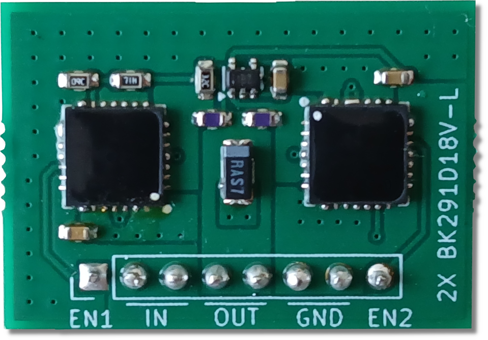
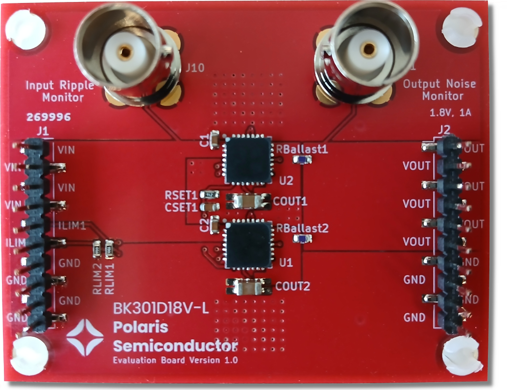
The circuit schematic in Figure A1 is an example of a parallel configuration of two BK291D18V devices. BK291D18V contains two optocouplers and is suitable for output voltages in the range of 1.2 V to 2.0 V. This ELR can be operated in three modes, “L”, “M”, or “LDO mode”, configured using the package pin connections. The mode dictates the input voltage range in which the regulator will operate most efficiently. Consult the device datasheet for additional information [1]. In the circuit design in Figure A1, the devices are configured in the “L” configuration. In this configuration, the two LEDs within are connected in parallel resulting in a lower turn on voltage, suitable for stepping typical single-cell Li-ion voltages to a regulated 1.8 V output, for example. For balancing the currents in the ELRs, a low-cost Texas Instruments TLV9001 rail-to-rail op-amp was chosen [2]. This part can operate on a single-sided supply to as low as 1.8 V and up to 5.5 V. The whole assembly fits into a board space of 2.7 cm² and can source up to 2 A of current. A basic, low-cost, 2-layer PCB design was used with 35 µm (1 oz/ft²) copper thickness. Sense resistors RS1 and RS2 were chosen to be 50 mΩ, giving a good balance of sensitivity and low ohmic loss. At maximum current (1 A per regulator), each 50 mΩ sense resistor drops 50 mV, so the regulators output 1.85 V to deliver the target 1.8 V at the board output. A photograph of the assembled board is shown in Figure 2.
Under continuous DC input conditions, the devices heat up by an amount depending on the dissipated power in the semiconductor chips, , and the thermal resistance between the semiconductors and the ambient. The thermal resistance, , is not a fixed value for a given package, but depends on many factors such as PCB design, board size, internal package layout, altitude, and more. However, it is still a useful figure of merit in this study to compare the impact of single and parallel operation, even though the absolute values are not directly transferable to other applications. The relationship between the junction and ambient temperatures [3] is given by:
Here is the ambient temperature and is the junction temperature. Since we cannot directly measure the junction temperatures of the chips within our packages, we obtain an approximate measure of the junction temperature by measuring the case temperature, , using a FLIR camera. We assume that all chips within the package have very similar junction temperature, so the thermal metric used to relate the junction temperature, , to the package surface temperature is , with the following relationship [3]:
In the QFN packages used for BK291D18V, the dice are physically separated from the top surface by only a thin region of plastic mold compound, which promotes a small value of . Furthermore, for packages with exposed die pads and operating under natural convection conditions, the dominant heat extraction path is through the die pad to the PCB, which has also been shown to lead to lower values of [3]. In our tests, performed under natural convection conditions, we assume is close to zero and therefore the difference in the top of the package temperature and the junction temperature of the chips inside is negligible.
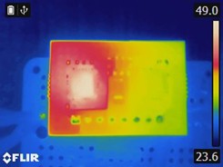
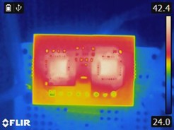
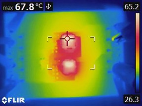
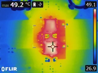
For the same board layout and load current, the operating temperature of the parallel regulators is considerably lower than the single regulator. This is shown in Figure 3 for a load current of 400 mA and an input voltage of 3.7 V. The paralleled configuration of Figure 3b also shows device temperatures are closely matched between the two regulators, confirming the output currents are closely matched. The total efficiency of the single and parallel configurations under these conditions is 65.7% and 65.9%, respectively, compared to the maximum theoretical efficiency of a linear regulator of 48.6% operating under identical conditions.
The fitted thermal resistance of the single ELR configuration is 59 °C/W, which reduces to 46 °C/W in the parallel configuration. As mentioned, these values are specific to the test board design—lower thermal resistances are possible using larger PCB areas, more copper layers, thicker copper pours, forced air cooling and so on. However, the relative comparison of thermal resistances clearly demonstrates the advantage of paralleling the chips. A further consideration for the parallel configuration is that, for a given output current, the current per ELR is approximately halved. Therefore, at high currents, losses due to device series resistance are substantially lower in the parallel case, reducing dissipated power levels for a given load current. The modeled thermal resistance of the single and parallel configurations is 59.9 °C/W and 49.8 °C/W, respectively, reproducing the improved thermal resistance available using ELRs in parallel. The measured case temperature for single and parallel connected ELRs is shown versus dissipated power in Figure 4a and versus load current is shown in Figure 4b.


The primary ELR senses the output voltage after the sense resistor, and therefore the load regulation is not adversely impacted by the inclusion of the sense resistors. However, the extra series resistance does have the effect of increasing the dropout voltage of the LDO inside BK291D18V, which in turn increases the turn on voltage of the ELR at high current relative to a standalone BK291D18V chip without a sense resistor. For a 1 A output current and 50 mΩ sense resistors, this corresponds to a 50 mV increase in dropout for the single ELR and 25 mV for the parallel ELRs, which is an additional consideration when specifying system voltage and current limits. The load regulation for single and parallel ELRs is shown in Figure 5 for an input voltage of 3.7 V. At low currents the load regulation is very similar. However, at high currents, the output voltage of the single ELR begins to fall as the device gets close to dropout. As expected, in the parallel configuration, dropout occurs at significantly higher current due to the current being shared between two ELRs and two sense resistors.

Another significant property of paralleled ELRs is that the output noise performance is improved relative to the single ELR case. There are two primary sources of self-generated noise in each ELR: the resistor divider and the bandgap voltage reference. The self-generated noise from each parallel-connected ELR is uncorrelated, meaning the random noise voltage generated by one ELR at any given instant has no relationship to the noise voltage being generated by another ELR at that same instant. In this case, it follows from the statistical treatment of random noise [4] that the total voltage noise output by parallel connected regulators scales in proportional to . Figure 6 shows the noise spectral density of BK291D18V-L in both single and parallel operation, with a clear reduction in output noise in the parallel case. The root-mean-square values of output noise are 98 µVRMS in parallel versus 148 µVRMS for the single device, integrated between 10 Hz to 100 kHz. The ratio of 66% between these values is close to the theoretical ratio of 70.1%.

Paralleling BT29 Series Step-Up ELRs
When paralleling boost-mode ELRs, such as BT291D50M, we can adopt a similar principle of current balancing as the BK291D18V case shown earlier. However, balancing the load currents across a sense resistor as shown in Figure 1b has a practical issue; if the op-amp supply is sourced from , then we no longer have sufficient supply headroom for the op-amp to function. This is because the inverting and non-inverting inputs derived from the ELR outputs will normally exceed in a boost device. If a higher voltage bias supply that exceeds the ELR output is available, then we can use it to supply the op-amp and proceed with a similar configuration to Figure 1b. However, in many practical cases, such as systems powered entirely by a Li-ion battery, no higher voltages are available and therefore we must modify our circuit.

Figure 7 shows an effective solution that can balance two boost mode ELRs using only the input supply voltage. Here, we are using the op amp to match the input current flowing into the primary and secondary ELRs, rather than matching the output currents. Since the potentials at the inverting and non-inverting terminals of the op-amp are very close to the supply voltage in this configuration, rail-to-rail operation of the op amp is essential; TLV9001 is a great candidate as it has a common-mode voltage range that can exceed the positive supply by 100 mV and a minimum supply voltage that is well within the minimum voltage range of BT291D50M. We can therefore use VIN to power both the op-amp and the ELRs up to the maximum supply voltage of TLV9001 of 5.5 V.
The circuit schematic in Figure A3 is an example of a parallel configuration of two BT291D50M devices. Each ELR can supply a maximum output current of 350 mA, enabling maximum output current and voltage of 700 mA and 5 V, respectively. A photograph of the assembled board is shown in Figure 8a and a thermal camera image of the board in operation under natural convection conditions is shown in Figure 8b. In this image, the input voltage is 3.7 V and the output current is 500 mA at nominally 5 V. The total efficiency of the parallel configuration under these conditions is 53%. The closely matched device temperatures verify the equivalent input currents to the ELRs.
The line regulation of the parallel boost converters is shown in Figure 9a, revealing a low output voltage variation of −0.69 %/A. The larger size of the parallel BT291D50M PCB compared to the parallel BK291D18V board results in a reduced thermal resistance, registering 20 °C/W for the paralleled boost regulator (Figure 9b). As with the parallel buck regulator topology, the inclusion of sense resistors negatively impacts the turn on voltage of the boost regulators. Figure 9c shows the voltage drop between the PCB IN pin and the input pins of the ELR versus input current, which includes the sense resistors and input channel PCB trace resistance. A line of best fit gives an estimated lumped series resistance of 26.9 mΩ, which results in an increase of the ELR turn on voltage by approximately 45 mV at a load current of 600 mA.


Paralleling Ultra-Low-Noise BK30 Series Step-Down ELRs
Extremely noise-sensitive applications increasingly require ultra-low noise DC power to achieve their target performance. This includes RF systems, precision analog applications, high-speed data serialization and deserialization (SerDes), high-end audio hardware, and many more. Our BK30 devices are built to provide exquisite ripple rejection and output noise performance, suitable for even the most extreme noise-sensitive applications, but with much higher efficiency than conventional LDOs. Paralleling our BK30 devices makes the output current scalable; this enables output current levels that compete with switching regulators but without the EMI drawbacks, and reduces the thermal dissipation challenges compared to using lossy but low-noise LDOs.
BK30 series chips support output currents up to 500 mA. The LDO inside the package is LT3045, which uses a 100 µA precision current source that is passed through an external resistor to generate a reference level for the internal error amplifier [5]. In a parallel configuration, the current sources of the individual devices are tied together to generate a single reference voltage, , common to each regulator. The worst case offset in compared to is 2 mV for each ELR. With this level of precision, paralleling requires only a low value ballast resistor to equalize the current in each ELR, and therefore an op-amp is no longer necessary. A simplified schematic drawing of two paralleled BK30 regulators is shown in Figure 10a. Note, since the current flowing in the set resistor is doubled with respect to the single ELR case, the value of the set resistor to produce a given output voltage is halved. The ballast resistor technique also makes it very straightforward to add more ELRs for even higher output currents, with the set resistor value decreasing for each additional resistor. For ELRs, this gives:
Although using ballast resistors is simple and low-cost, there is a trade-off in accuracy and parasitic loss since they introduce a series resistance between the ELR and the load. Higher values of ballast resistance improve the current balancing at the expense of increased losses. Figure 10b shows the calculated deviation in output voltage assuming a 1 A output current for two parallel BK301D18V ELRs. The current matching, assuming the worst case offset in to , is also shown. A ballast resistance of 50 mΩ was used in the example PCB design in this note, which provides a worst-case current mismatch below 10% and less than 1.3% deviation in output voltage at maximum current.


The circuit schematic in Figure A5 shows a detailed design of two parallel BK301D18V devices on a low cost, 2 layer PCB. BK301D18V is from the BK30 ultra-low noise series, featuring a wider 0–2.0 V output range while maintaining the same input voltage ranges and operating modes as BK291D18V. A photograph of the assembled board is shown in Figure 10c and a thermal camera image of the board in operation under natural convection conditions is shown in Figure 10d. In this image, the input voltage is 3.7 V and the output current is 1 A at a nominal output voltage of 1.8 V. The total efficiency of the parallel configuration under these conditions is 64.0%.
LT3045 has a convenient feature for monitoring the current in the pass transistor using the ILIM pin, which sources current proportional (1:500) to the ELR’s pass transistor. The pin serves dual purposes: programmable current limiting and current monitoring. The current limit is set by connecting a resistor () between ILIM and GND, limiting the pass transistor current to a maximum of . For current monitoring without external limiting, values of 249 Ω or 280 Ω keep the ILIM pin voltage within its 0–300 mV monitoring range at maximum current while allowing the internal current limit to remain active. If current monitoring and external limiting are not needed, simply tie ILIM to GND.
Figure 11a plots the input current—approximated using the ILIM pin monitoring strategy—of the two parallel ELRs versus load current, demonstrating that the ELR currents are closely matched and the total input current (ELR1+ELR2) is significantly lower than the output current due to the optocoupler enhancement effect in the ELRs. As expected, the load regulation of the output voltage is dominated by the ballast resistance (Figure 11b). The slope of the output voltage corresponds to a total resistance of 28.6 mΩ, which also includes the PCB trace resistance as well as the load and temperature regulation properties of LT3045.


Conclusions
In this application note, we have described the principles of current balancing in parallel connected ELRs. Parallel ELR connections are a robust way to scale the output current for power hungry applications, while offering additional benefits in thermal dissipation and reduced output noise. In each case, however, a small penalty in either turn-on voltage or output load regulation exists due to the inclusion of additional resistors.
We showed a low-cost and compact op-amp based configuration that supports parallel buck and boost circuits using BK29 and BT29 series parts. We also showed an ultra-low noise application using BK30 series parts that use an extremely simple ballast resistor technique, requiring only one additional, small-footprint resistor per regulator. These circuits are useful building blocks for noise-sensitive, high-current applications where the noise output from switching regulators is highly problematic, but require better thermal and power consumption performance than is available using conventional linear regulators.
Appendix
BK29 Step-Down Parallel Demo Schematic

BK29 Step-Down Parallel Demo Bill of Materials
| ID | Description | Part | Manufacturer |
|---|---|---|---|
| C1, C2, C4 | 0.1 µF ceramic X7R | CL10B104KB8NNWC | Samsung Electro-Mechanics |
| C3 | 47 µF tant poly | T527I476M010ATE200 | KEMET |
| R1 | 5.36 kΩ 0.5% 1/16W | RR0816P-5361-D-71H | Susumu |
| R2 | 12.1 kΩ 0.5% 1/16W | RR0816P-1212-D-09C | Susumu |
| R3 | 21 kΩ 0.5% 1/16W | RR0816P-2102-D-32C | Susumu |
| R4, R5 | 50 mΩ 1% 1/4W | UR73D1JTTD50L0F | KOA Speer Electronics, Inc. |
| U1, U2 | 1.2–2V ELR | BK291D18V | Polaris Semiconductor |
| U3 | Operational Amplifier | TLV9001IDCK | Texas Instruments |
BK29 Step-Down Parallel Demo Board Layout


BT29 Step-Up Parallel Demo Schematic

BT29 Step-Up Parallel Demo Bill of Materials
| ID | Description | Part | Manufacturer |
|---|---|---|---|
| C1, C3, C5 | 0.1 µF ceramic X7R | CL10B104KB8NNWC | Samsung Electro-Mechanics |
| C2, C4 | 22 µF tant poly | TAJA226K010RNJ | KEMET |
| J1, J2 | CONN HEADER SMD 2.54MM | HDR100IMP40M-G-V-SM | Chip Quik Inc. |
| R1, R4 | 14.7 kΩ 0.5% 1/16W | RR0816P-1472-D-17C | Susumu |
| R2, R3 | 4.87 kΩ 0.5% 1/16W | RR0816P-4871-D-67H | Susumu |
| R7, R8 | 50 mΩ 1% 1/4W | UR73D1JTTD50L0F | KOA Speer Electronics, Inc. |
| R9, R10 | 10.2 kΩ 0.5% 1/16W | RR0816P-1022-D-02C | Susumu |
| R11 | 21 kΩ 0.5% 1/16W | RR0816P-2102-D-32C | Susumu |
| U1, U2 | 5V BOOST ELR | BK291D18V | Polaris Semiconductor |
| U3 | Operational Amplifier | TLV9001IDCK | Texas Instruments |
BT29 Step-Up Parallel Demo Board Layout


BK30 Step-Down Parallel Demo Schematic

BK30 Step-Down Parallel Demo Bill of Materials
| ID | Description | Part | Manufacturer |
|---|---|---|---|
| C1, C2, CSET1 | 4.7 µF ceramic X7R | GRM188Z71C475KE21J | Murata Electronics |
| COUT1, COUT2 | 10 µF ceramic X7R | CL31B106KBHNNNE | Samsung Electro-Mechanics |
| J1, J2 | CONN HEADER SMD 2.54MM | HDR100IMP40M-G-V-SM | Chip Quik Inc. |
| J10, J11 | CONN BNC RCPT | 112404 | Amphenol RF |
| RBALLAST1, RBALLAST2 | 50 mΩ 1% 1/4W | UR73D1JTTD50L0F | KOA Speer Electronics, Inc. |
| RLIM1, RLIM2 | 280 Ω 0.5% 1/16W | RR0816P-2800-D-44A | Susumu |
| RSET1 | 9.1 kΩ 0.1% 1/10W | RG1608P-912-B-T5 | Susumu |
| U1, U2 | 0–2V ELR | BK301D18V | Polaris Semiconductor |
BK30 Step-Down Parallel Demo Board Layout


References
- BK291D18V: 1.0A output adjustable voltage regulator. Polaris Semiconductor; Datasheet available upon request, 2025.
- TLV900x low-power, RRIO, 1-MHz operational amplifier for cost-sensitive systems. Texas Instruments; Datasheet SBOS833R, 2021.
- D. Edwards and H. Nguyen, “Semiconductor and IC package thermal metrics.” Texas Instruments; Application Note SPRA953D, 2024.
- S. Ziel, “Parallel LDO architecture design using ballast resistors.” Texas Instruments; Technical White Paper SBVA100, 2022.
- LT3045 20V, 500mA, ultralow noise, ultrahigh PSRR linear regulator. Analog Devices; Datasheet, 2022. Available: https://www.analog.com/media/en/technical-documentation/data-sheets/lt3045.pdf
Ready to design it in?
Request evaluation samples, detailed datasheets, and SPICE models — an engineer answers, not a sales funnel.